


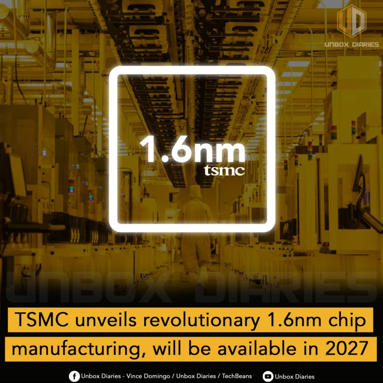
TSMC has unveiled a groundbreaking 1.6-nanometer (nm) chip manufacturing process, dubbed A16. This represents a significant leap forward, offering not only transistor miniaturization but also a revolutionary backside power delivery network.
A16: Power Efficiency and Performance on Steroids
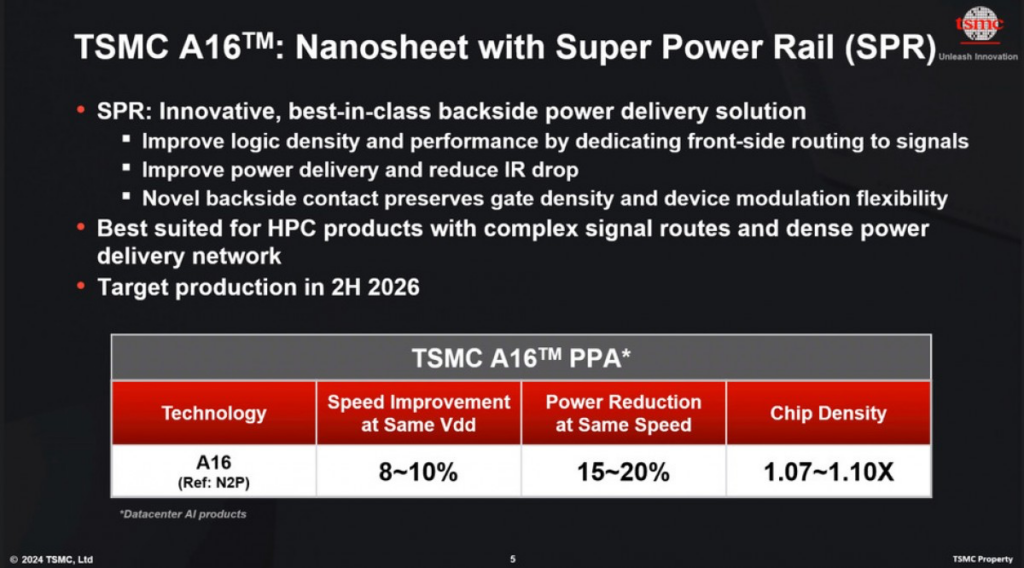
The A16 process builds upon gate-all-around nanosheet transistors, similar to TSMC’s upcoming 2nm N2, N2P, and N2X architectures. However, A16 takes it a step further. It delivers an impressive 10% increase in clock speeds at the same voltage and a remarkable 20% reduction in power consumption compared to previous nodes, all while potentially enabling up to 10% more transistors in a chip design.
The Secret Weapon: Backside Power Delivery
The true game-changer might be the backside power delivery network. By moving power rails to the back of the chip, A16 frees up valuable space on the front for more signal rails. This translates to significant benefits for processors demanding complex wiring and dense power networks, particularly in AI and high-performance computing (HPC) applications. TSMC’s Super Power Rail (SPR) technology further optimizes this power delivery system.
Looking Ahead: A 2026 Reality
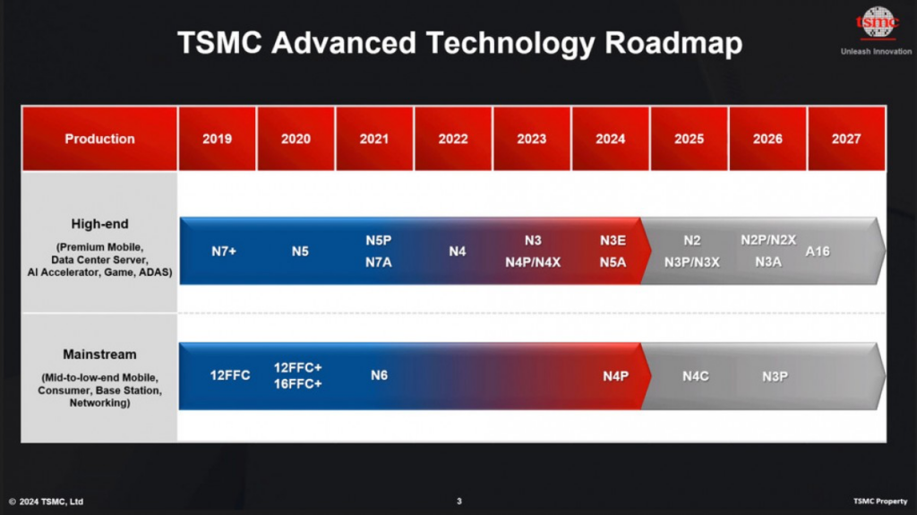
With a targeted production timeline for the second half of 2026, the first consumer products featuring this revolutionary technology are expected to hit the market sometime in 2027.